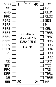
Pinout of CDP6402 | There are such UARTs as CDP6402, AY-5-1015 / D36402R-9 and compatibles. They differ from the 8250 line and their prototypes as they have pinouts for plugging to necessary logical levels instead of data bus, this suits well for the case when the microprocessor is not used. E.g. you want to plug ADC0804 (Analog to Digital Converter) to UART,
or want to connect a LCD Display to the Serial Line. These common devices use a 8 bit parallel data bus.
The CDP6402's Control Register is made up of Parity Inhibit (PI), Stop Bit Select (SBS), Character Length Select (CLS1 and 2) and Even Parity Enable (EPE). These pinouts can be disabled by Control Register Load (CRL), if you want to switch this pinout to high level, the changes done with the help of these pinouts take place immediately. |
| Pin Number | Abbr. | Full Name | Notes |
| Pin 1 | VDD | + 5v Supply Rail |
| Pin 2 | NC | Not Connected |
| Pin 3 | GND | Ground |
| Pin 4 | RRD | Receiver Register Disable | When driven high, outputs RBR8:RBR1 are High Impedance. |
| Pin 5:12 | RBR8:
RBR1 | Receiver Buffer Register | Receiver's Data Bus |
| Pin 13 | PE | Parity Error | When High, A Parity Error Has Occurred. |
| Pin 14 | FE | Framing Error | When High, A Framing Error Has Occurred. i.e. The Stop Bit was not a Logic 1. |
| Pin 15 | OE | Overrun Error | When High, Data has been received but the nData Received Reset had not yet been activated. |
| Pin 16 | SFD | Status Flag Disable | When High, Status Flag Outputs (PE, FE, OE, DR and TBRE) are High Impedance |
| Pin 17 | RRC | Receiver Register Clock | x16 Clock input for the Receiver Register. |
| Pin 18 | nDRR | Data Received Reset | Active Low. When low, sets Data received Output Low (i.e. Clears DR) |
| Pin 19 | DR | Data Received | When High, Data has been received and placed on outputs RBR8:RBR1. |
| Pin 20 | RRI | Receiver Register In | RXD - Serial Input. Connect to Serial Port, Via RS-232 receiver. |
| Pin 21 | MR | Master Reset | Resets the UART. UART should be reset after applying power. |
| Pin 22 | TBRE | Transmitter Buffer Register Empty | When High, indicates that Transmitter Buffer Register is Empty, thus all bits including the stop bit have been sent. |
| Pin 23 | nTBRL | Transmitter Buffer Load / Strobe | Active Low. When low, data present on TBR8:TBR1 is placed in Transmitter Buffer Register. A Low to High Transition on this pin, then sends the data. |
| Pin 24 | TRE | Transmitter Register Empty | When High, Transmitter Register is Empty, thus can accept another byte of data to be sent. |
| Pin 25 |
TRO |
Transmitter Register Out (TXD) |
TXD - Serial Output. Connect to Serial Port, Via RS-232
Transmitter. |
| Pin 26:33 |
TBR8:
TBR1 |
Transmitter Buffer Register |
Data Bus, for Transmitter. Place Data here which you want to
send. |
| Pin 34 |
CRL |
Control Register Load |
When High, Control Register (PI, SBS, CLS2, CLS1, EPE) is
Loaded. Can be tied high, so changes on these pins occur
instantaneously. |
| Pin 35 |
PI |
Parity Inhibit |
When High, No Parity is Used for Both Transmit and Receive. When
Low, Parity is Used. |
| Pin 36 |
SBS |
Stop Bit Select |
A High selects 2 stop bits. (1.5 for 5 Character Word Lengths) A
Low selects one stop bit. |
| Pin 37:38 |
CLS2:
CLS1 |
Character Length Select |
Selects Word Length. 00 = 5 Bits, 01 = 6 Bits, 10 = 7 Bits and
11 = 8 Bits. |
| Pin 39 |
EPE |
Even Parity Enable |
When High, Even Parity is Used, When Low, Odd Parity is
Used. |
| Pin 40 |
TRC |
Transmitter Register Clock |
16x Clock input for Transmitter. | Pin Description for CDP6402, AY-5-1015 / D36402R-9 and compatible
UART's
However there is one drawback of using these chips comparing to 8250
chips, as there is no Programmable Baud Rate Generator or any other means
of changing speed for direct chip connection. Akthough there are Baud Rate Generator
Chips such as the AY-5-8116, a more cheaper (and common)
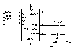
alternative is the 74HC4060 14-bit Binary Counter and Oscillator.
The 74HC4060, being a 14 bit binary counter/divider only has pinouts for some of it's stages. Only Q4 to Q14 is available for use as they have
external connections. This means higher Baud Rates cannot be obtained from
common crystals, such as the 1.8432 Mhz and 2.4576 Mhz. The UART requires
a clock rate 16 times higher than the Baud Rate you will be using. eg A
baud rate of 9600 BPS requires an input clock frequency of 153.6 Khz.

Baud Rate Generator using a 74HC4060 |
| Output |
1.8432Mhz |
2.4546Mhz |
| Out 2 |
115.2 KBPS |
153.6 KBPS |
| Q4 |
7200 BPS |
9600 BPS |
| Q5 |
3600 BPS |
4800 BPS |
| Q6 |
1800 BPS |
2400 BPS |
| Q7 |
900 BPS |
1200 BPS |
| Q8 |
450 BPS |
600 BPS |
| Q9 |
225 BPS |
300 BPS | Possible Baud Rates using a
74HC4060 |
The 1.8432 Mhz crystal gives some unfamiliar Baud Rates. While many of
these won't be accepted by terminal programs or some hardware, they are
still acceptable if you write your own serial programs. For example the
PC's baud rate divisor for 7200 BPS is 16, 3600 BPS is 32, 1800 BPS is 64
etc. If you require higher speeds, then yuo can connect the UART
to the OUT2 pin. This connection utilizes the oscillator, but no
frequency division is applied here. Using OUT2 with a 1.8432 Mhz crystal connected
gives a baud rate of 115,200 BPS. The CMOS CDP6402 UART can handle up to
200 KBPS at 5 volts, however your MAX-232 may be limited to 120 KBPS, but
is still within range.
| |